SEM is a staple within the materials research community and is a crucial tool for surface analysis within a broad array of disciplines such as chemistry, physics, biology, and engineering. Contrary to a light microscope, which typically uses light in the visible range to investigate the surface of the sample, SEM uses electrons. This has several advantages.
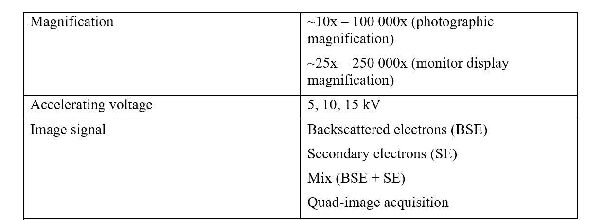
The electrons make it possible to achieve a much higher level of magnification. Our instrument can acquire images in the magnification range from ~20 to 100 000x. The backscatter electrons (BSE) also give us a contrast between different elements, for example, making it possible to identify different composition domains on the surface. We can also collect the secondary electrons (SE), which, because of their elastic interaction with the surface, allows for topographic contrast.
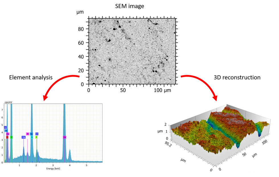
By taking advantage of the characteristic X-rays emitted, because of electrons in-elastically interacting with the surface, we can do quantitative energy-dispersive X-ray spectroscopy (EDX). With EDX, we can get quantitative element composition, achieving an accuracy of approximately 0.1 % (sample dependent) of the sample.
Furthermore, the SEM has a 4-segment BSE detector, which allows for 3D visualization of the surface. By acquiring a segmented image, a 4-quadrant reconstruction is performed (Hitachi 3D Map software), resulting in a 3D model of the surface. This adds another dimension to our SEM imaging, making it possible to acquire metrological data of the surface, including contour analysis. This is beneficial in our work with dental materials when analyzing surface treatments and abrasion effects.
A variety of samples can be analyzed, with the instrument being able to accommodate samples up to 5 cm in thickness and 8 cm in diameter. The current SEM can measure at three different voltages, 5, 10, and 15 eV, with four different beam currents at each voltage.
We can also alter the vacuum of the measurement chamber to reduce charging effects for low conducting samples. Beyond this, we can manipulate samples for optimal imaging, including surface coating (e.g., gold and carbon) for improved surface conductivity, and dehydrate and fixate biological samples.